- Home
- Technology Groups
- Competence Center for Micro- and Nanotechnologies
- Research results
- Production of 3D Nanostructures for Innovative Biosensors
Production of 3D Nanostructures for Innovative Biosensors

23.04.2018
For the first time, researchers at Leibniz IPHT have succeeded in using atomic layer deposition to create complex three-dimensional nanoscale architecture without the assistance of pre-structured 3D templates. The simple two-stage process enables the production of large active sensor surfaces at lower cost, which is particularly interesting for applications in the life sciences.
By: Mario Ziegler // Dana Cialla-May // Sezin Yüksel // Sebastian Goerke // Uwe Hübner
Three-dimensional (3D) nanostructures exhibit unprecedented properties in interaction with light due to their very small structure size and increased interaction medium. Through specific application of these properties, novel sensors and detection methods for the life sciences can be developed, the effects of which are further enhanced by the 3D architecture. However, the production of 3D micro and nanostructures still proves very difficult, despite countless bottom-up (e.g., self-organizing monolayers) and top-down processes (e.g., classical photolithography). After an extensive process chain, many approaches lead to a single complex structure. This makes the processes inflexible and sometimes very costly. An application of these structures in the life science sector is, therefore, not feasible. The procedure developed in cooperation between IPHT and FSU Jena makes it possible to produce 3D nanostructures by means of a simple two-stage process. The final nanoscale architecture can be individually adjusted by several parameters. This enables the production of different structures for a wide range of applications.
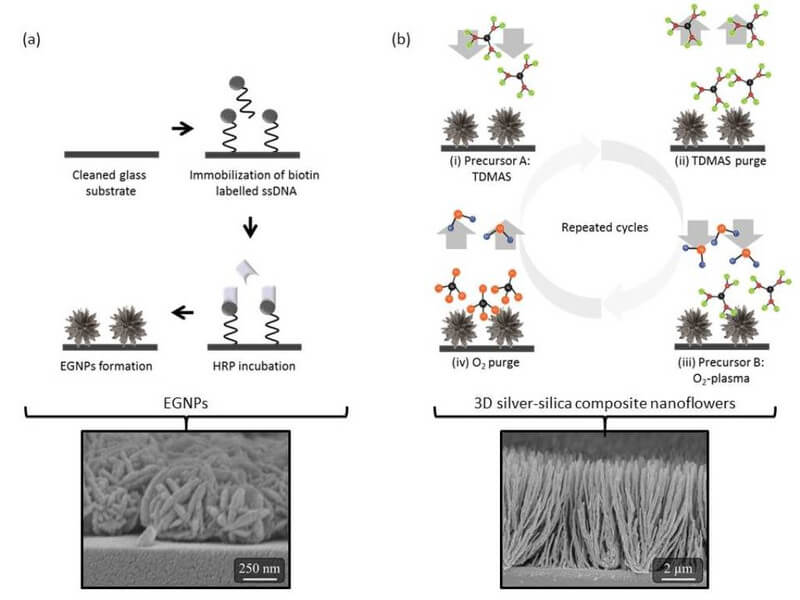
Figure 1 shows schematically the process flow for the production of 3D nanostructures. In the first step, a precious metal (gold, silver, or platinum) is deposited on a substrate. This can be achieved by both nanoparticle synthesis and physical vapor deposition [1]. In a second step, the previously deposited precious metal is coated with silicon dioxide (SiO2) by means of plasma-enhanced atomic layer deposition (PEALD). In contrast to classical ALD, the parameters of the deposition process are modified in such a way that the precious metal forms a metastable phase. The metastable phase occurs for a limited time due to the cyclic behavior of the ALD process. As a result, the precious metal and a metastable phase of the precious metal are alternately present in the ALD reactor at different times. While the coating of the precious metal leads to a planar (2D) deposition, the coating of the metastable phase results in a transformation of the surface to 3D architecture.
This is due to the fact that plasma particles react with the substrate in the plasma section of the ALD process (see Fig. 1b III). This leads to an increase in volume in the first atomic layers of the substrate surface. The substrate is partially raised by the increase in volume and begins to form porous structures. In contrast to structural transformations, however, the increase in volume is a reversible process due to the metastable phase, during which the plasma particles built into the substrate surface are released again. By selecting the appropriate parameters in the ALD process, various structures can be generated on this basis (see Fig. 2).
To assess the performance for biophotonic applications, the structures were analyzed in a measurement setup for surface-enhanced Raman spectroscopy (SERS) [2]. It was found that the 3D nanostructures did not show significant Raman bands (see Fig. 3a). They can thus be used as an ideal template for SERS measurements, although a plasmonically active material suitable for the examination has to be deposited on the structures first (see Fig. 3b). The measurements also exhibited a very good reproducibility of the results across the entire chip area, as well as from batch to batch. The SERS-active structures were wetted with riboflavin (see Fig. 3c) in order to estimate the applicability of the structures for micro concentrations. Riboflavin was measured in the range from 5 µM to 0.025 µM with a reliable detection limit of 50 nM.
Funded by: BMBF, DFG


