- Home
- Research
- Functional Interfaces
- Work-Groups
- Photonic Thin Film Systems
Photonic Thin Film Systems
The research group is engaged in the investigation of semiconductor thin films and nanostructures, in particular on the basis of silicon and transparent conductive materials for photonic components such as optical sensors on various carrier materials. The research of the group is based on a broad spectrum of physical and wet chemical coating and deposition processes (e.g. chemical vapor deposition (CVD), electron beam evaporation (EBE), atomic layer deposition (ALD), sputtering and inkjet printing). These approaches are combined with laser processes for the crystallization of semiconductors and the production of nanoparticles. This addresses applications in the field of smart textiles, environmental and medical technology. The research group investigates solutions for optical detection systems in biomedical imaging and analytical spectroscopy as well as concepts for the realization of energy-autonomous systems for individualized health monitoring.

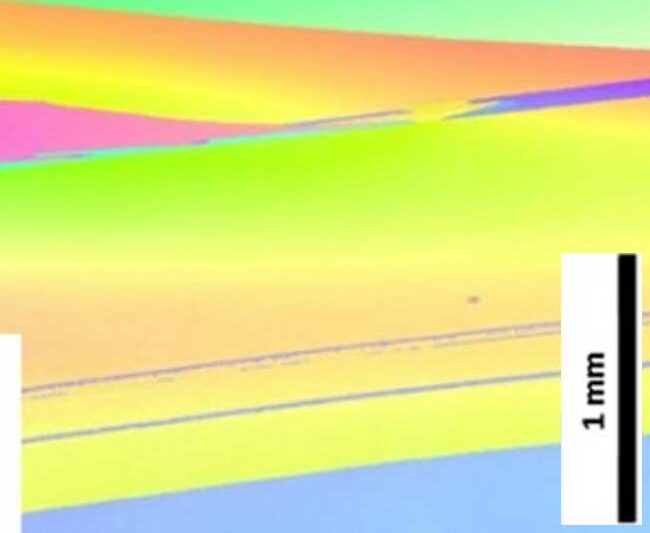
Laser crystallized silicon thin film

Thin-film solar cells on textiles
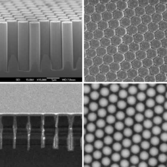
Silicon nanowire array with core-shell structure
Selected Research Topics
- Silicon-based thin-film solar cells on textiles and low-cost substrates
- Laser-assisted nanoparticle production from metal alloys for plasmonics and catalysis
- Highly transparent multi-electrode arrays (MEA) for biomedical imaging using super-resolution microscopy (SRM)