Sn_SERS
Development and atomic and electronic structure characterization of functional Sn/SnOx surfaces for SERS-based misfolded protein analysis
Runtime: 01.04.2021 - 31.12.2024
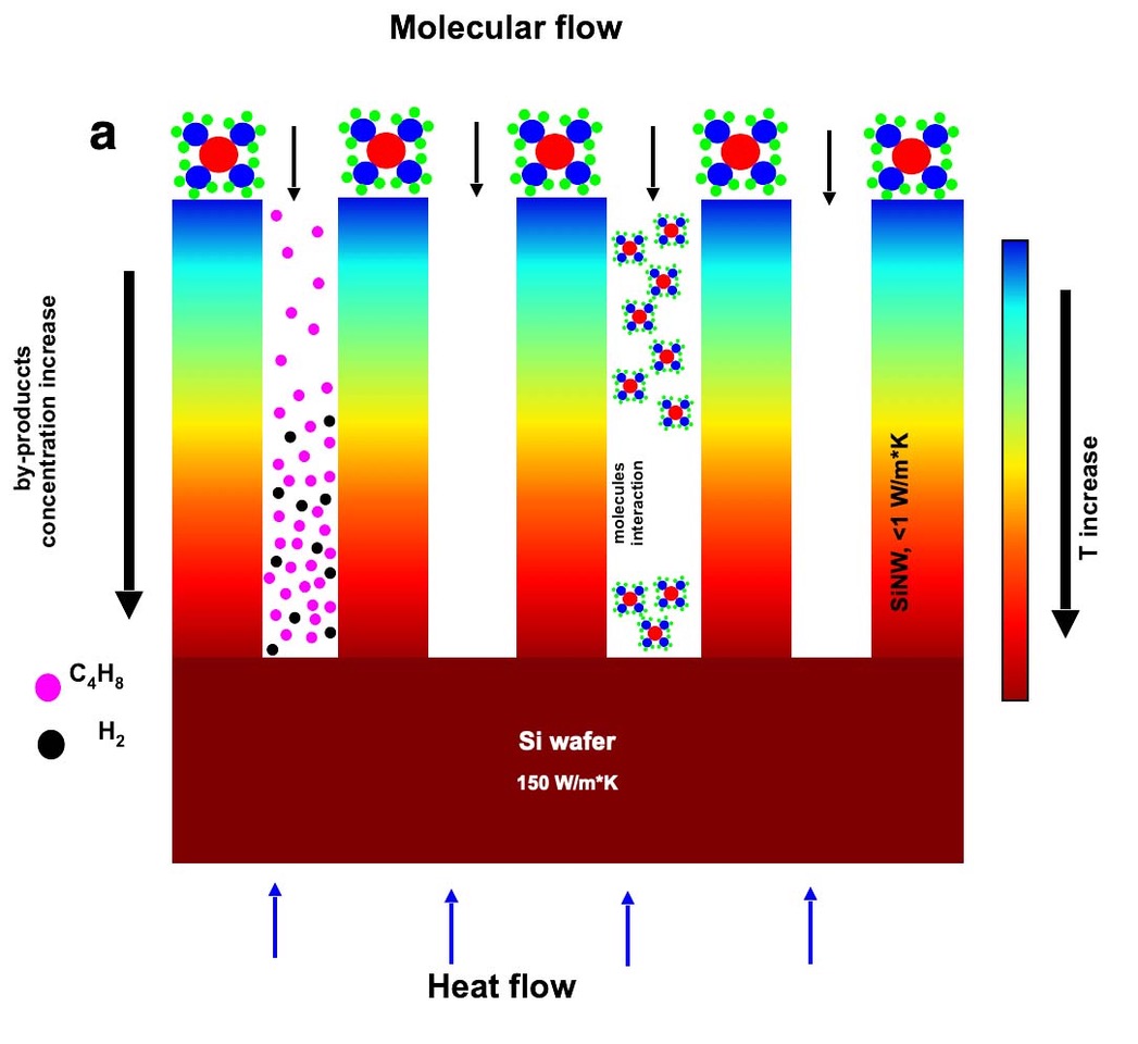
Sn/SnOx nanostructured surfaces are very promising for different applications since their state of condensed matter is located between isolated atoms (or small molecules) and the bulk phase. In contrast to the inherent properties of bulk material, the nanomaterial with the same chemical composition shows novel properties, depending on the medium in which they are embedded. The inherent advantages of nanostructured materials can be improved by combining two phases with distinct properties to produce Sn-based nanocomposites as proposed in the framework of this research project. Functional Sn-based nanostructures embedded in a SiNWs matrix have some advantages and offer attractive options due to their chemical and mechanical stability, low cost production, and improved optical and catalytic properties. In this respect, the targeted scientific breakthrough of the proposed project will be the controlled growth of tin-based thin films on nanostructured silicon and quartz surfaces for biophotonic applications. The local electric field enhancement factor of Sn/SnOx plasmonic nanostructures and the surface stability of such surfaces produced by chemical or physical vapor deposition techniques have not been studied yet. For this reason, the characterization of long-term stability and surface composition are highly important, especially with regard to the development of new application strategies. A top-down wet-chemical approach will be used for the pre-patterning of silicon surfaces followed by intersectioning with functional tin oxide layers. For the formation of the tin-based plasmonic active surfaces metalorganic chemical vapor deposition using tin(II) and tin(IV) volatile alkoxide precursors and metallic tin magnetron sputtering will be applied. The characterization of the obtained plasmonic structures will be performed with different surface sensitive analytical methods. The results will be complemented by theoretically modeling growth processes and plasmonic properties. Thereby, an optimized procedure for Sn/SnOx nanostructured surfaces will be developed and established. A precise and detailed analysis of the atomic and electronic structure as well as the physico-chemical state of the formed surfaces and interfaces will be achieved by using the following techniques: XANES (X-ray Absorption Near Edge Structure), XPS (X-ray Photoelectron Spectroscopy), and PEEM (Photo Emission Electron Microscopy) using large-scale facilities at BESSY II synchrotron storage ring at HZB Berlin will be applied to characterize the surface and achievable interfaces. Furthermore, with this technique it will be possible to investigate the atomic and electronic structure as well as the physico-chemical state of the silicon matrices before and after composite formation with unique non-destructive depth profiling. All methods will be applied in surface and bulk sensitive modes supplemented by computer modeling and electronic structure ab-initio calculations of the most important possible phases. The ex-situ and in-situ UHV modification of the localized nanostructures will allow to extend the understanding of material properties and stability. In the proposed bilateral research project the plasmonic activity of Sn/SnOx substrates will be exploited in surface-enhanced Raman spectroscopy (SERS) experiments on protein-related compounds. Using excitation laser wavelengths in the visible down to the deep-UV spectral region, the achieved spectroscopic data will provide new insights into the molecular structure of amyloid fibrils and their precursors. The proposed bilateral project thus covers the entire range from the development and characterization of novel plasmonic tin-based surfaces to their application for socially relevant topics.
This project is funded by the German Research Foundation (DFG)
Partners