- Home
- Research
- Quantum Systems
- Projects
- SuperLSI
SuperLSI
Runtime: 01.01.2022 - 31.12.2024
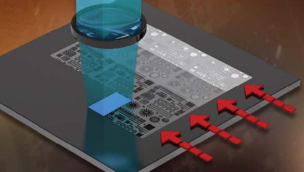
One of the most important core competencies in the context of second-generation quantum technologies based on superconducting quantum systems is the reproducible production of corresponding functional components and complete quantum circuits with the necessary controllable quality parameters. These include high-quality interfaces and surfaces, excellent layer quality, avoidance of any contamination, precise layer thickness control, and a very precise definition of the structures.
At the Leibniz-IPHT, new coating and structuring processes are being researched and tested as part of SuperLSI, which are specially tailored to superconducting quantum circuits with a focus on reproducibility, scalability, and application relevance. For this purpose, innovative processes and technologies for wafer-scale deposition of high-purity and granular aluminum, other superconducting materials (e.g. Nb, Ta), and suitable dielectrics on the one hand, and low-damage etching processes on an atomic layer basis, on the other hand, are being researched, realized and demonstrated. The combination of these processes and materials enable long coherence times on one hand and specific functionalities like high inductances and complex wiring on the other hand. This work takes a central position in the SuperLSI project and enables the implementation of innovative processes for manufacturing of superconducting quantum circuits.
The project SuperLSI is granted by BMBF under grant no. 13N16258 via VDI within the framework of the call „Enabling Technologies for Quantum Technologies“.
Partners